QCORE Seminar Series · November 5, 2025
Featuring Dr. Andrew Lingley, Manager
📄 Access the full slide deck (PDF)
Why We Hosted This Talk
At QCORE, one of our goals is to showcase the technologies that quietly shape modern research and industry. Some technologies are highly visible—telescopes, satellites, and large scientific instruments. Others operate behind the scenes, powering nearly every device we use without most people ever seeing how they work.
Microfabrication is one of those invisible engines.
From sensors to photonics to biomedical devices to quantum components, microfabrication forms the foundation for countless innovations. Yet even within research communities, the fabrication process often feels like a black box. People see the final chip, sensor, or device, but not the highly structured sequence of design, patterning, deposition, etching, and inspection that makes it possible.
That’s why we invited Dr. Andrew Lingley, Manager of the Montana Microfabrication Facility (MMF), to give the QCORE audience a clear and practical introduction to microfabrication—what it is, why it matters, and what it actually looks like to build functional structures at the micron and nanometer scale.
About the Speakers

Dr. Andrew Lingley
Dr. Andrew Lingley is the Manager of the Montana Microfabrication Facility (MMF). He oversees cleanroom operations, tool maintenance, process development, training, and research support across a wide range of micro- and nanoscale fabrication methods. His work enables students and researchers to move from concept to prototype through hands-on fabrication, testing, and iterative process refinement.
MMF operates under the leadership of Dr. David Dickensheets, Director of the facility.
Opening the Talk: Microfabrication Is Everywhere—But Rarely Seen
Andrew opens with a simple observation: microfabrication is embedded in modern life, but most people rarely think about it. Any device containing chips, sensors, microscopic structures, or precision-patterned surfaces depends on fabrication techniques that occur in controlled environments far removed from everyday experience.
He explains that microfabrication is not just about “making small things.” It is about building structures that behave in predictable ways when scaled down—structures that can guide light, detect motion, process electrical signals, or interact with biological systems.
In many ways, microfabrication is the enabling layer beneath modern science and engineering. Without it, much of the technology surrounding us would not exist.
A Brief Historical Context: How We Got Here
To help the audience appreciate why microfabrication matters, Andrew briefly steps back and connects the field to the history of semiconductor development. He describes how fabrication methods evolved alongside the electronics industry, moving from early transistor development toward modern integrated circuits.
As devices became smaller and more complex, fabrication became less like traditional machining and more like layered construction—building features through repeated cycles of patterning, material deposition, and etching. The tools became more specialized, the tolerances tighter, and the environments cleaner.
This historical framing helps explain why microfabrication is often described as an “invisible industry.” The products are visible, but the process is highly specialized, expensive, and physically inaccessible to most people.
Inside MMF: A Cleanroom Designed for Precision
Andrew then brings the discussion into the Montana Microfabrication Facility itself. He explains that MMF operates within controlled cleanroom environments—spaces where air filtration, airflow patterns, clothing requirements, and procedural discipline all exist for one reason: contamination control.
In microfabrication, dust is not an inconvenience. A single particle can destroy a pattern, disrupt an etch, block a feature, or cause a device to fail. Because the structures being fabricated may be only microns—or even nanometers—wide, even a speck invisible to the human eye can become catastrophic.
Andrew emphasizes that cleanroom work is not simply about equipment. It is about behavior. Students must learn how to gown properly, handle wafers safely, avoid static discharge, and move through the cleanroom without introducing particles. Cleanroom discipline is a skill, and it becomes part of the fabrication process itself.
Microfabrication as a Process Ecosystem
One of Andrew’s key points is that microfabrication is not a single tool or a single step. It is a process ecosystem.
Each fabrication step depends on the success of the one before it. A small misalignment early in the process can cascade into a complete failure later. A film deposited with the wrong stress profile can warp a mechanical structure. A rushed lithography step can destroy an entire wafer.
Because of this, microfabrication trains a particular mindset: careful, methodical, documentation-driven work. It is unforgiving, but it is also deeply educational. In Andrew’s view, the cleanroom is one of the best environments for teaching students how real engineering is done—through precision, iteration, and disciplined troubleshooting.
How Microfabrication Works: The Repeating Cycle
Andrew walks the audience through the general structure of a fabrication cycle. While every device has its own recipe, most microfabrication workflows follow a repeating pattern:
The process begins with a substrate, often silicon, glass, quartz, or polymers depending on the application. A thin film or resist is applied and prepared for patterning. A pattern is exposed and developed, then transferred into the material through etching or deposition.
And then the cycle repeats:
pattern → etch → measure → adjust → repeat
He emphasizes that fabrication is iterative by nature. Even experienced researchers rarely get a process perfect on the first attempt. Devices are built through cycles of testing, refinement, and incremental improvement.
The “Rectangle Rule”: A Teaching Shortcut That Works
One of the most memorable parts of Andrew’s seminar is the way he describes teaching microfabrication fundamentals.
He explains that for many students, microfabrication feels overwhelming because it involves so many tools, chemicals, and abstract process steps. But a simple design principle helps make it approachable:
Start with a rectangle.
Many devices—waveguides, channels, electrodes, MEMS structures—begin as patterned regions defined by straight edges. By learning how to successfully print, develop, and etch a rectangle, students learn many of the core principles of lithography, alignment, etch behavior, and process control.
This simple approach turns microfabrication into something teachable and repeatable, rather than mysterious.
Lithography: Turning an Idea Into a Pattern
Andrew highlights one of MMF’s major capabilities: Electron Beam Lithography (EBL).
Unlike traditional lithography, which uses masks and light exposure, EBL uses a focused electron beam to directly write patterns onto a resist. This enables extremely small features—structures at the nanometer scale—that would be difficult or impossible to create with conventional masks.
He explains that EBL opens the door to advanced research applications, including photonics, nano-optics, and quantum devices.
But he also emphasizes that EBL introduces its own challenges. Resist chemistry behaves differently under electron exposure, insulating substrates can accumulate charge, and write times can be long. Stable beam currents and careful parameter tuning become essential.
EBL is not just a tool—it is a discipline.
Electron Beam Lithography: When Masks Aren’t Enough
Andrew highlights one of MMF’s major capabilities: Electron Beam Lithography (EBL).
Unlike traditional lithography, which uses masks and light exposure, EBL uses a focused electron beam to directly write patterns onto a resist. This enables extremely small features—structures at the nanometer scale—that would be difficult or impossible to create with conventional masks.
He explains that EBL opens the door to advanced research applications, including photonics, nano-optics, and quantum devices.
But he also emphasizes that EBL introduces its own challenges. Resist chemistry behaves differently under electron exposure, insulating substrates can accumulate charge, and write times can be long. Stable beam currents and careful parameter tuning become essential.
EBL is not just a tool—it is a discipline.
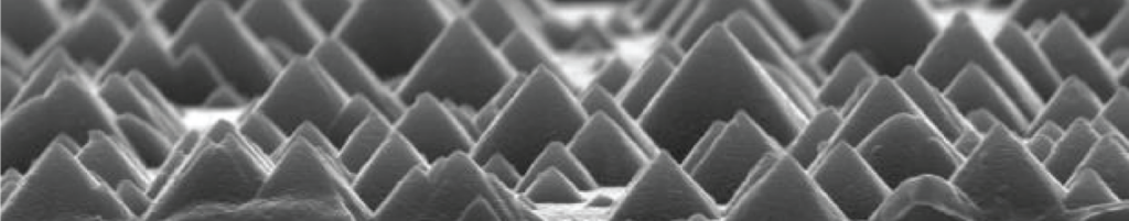
Etching and Deposition: Managing Matter Layer by Layer
Once patterns exist, they must be transferred into real materials. Andrew discusses etching—both wet and dry methods—as the process of removing material to create depth and shape.
He also describes deposition tools that add metals, oxides, nitrides, and multilayer films. Each material has its own behavior and “personality.” Some adhere only with specific adhesion layers, some develop internal stress that bends structures, and others require highly controlled deposition conditions.
Microfabrication, Andrew explains, is not just about building. It is about managing matter in thin layers, where microscopic deviations can produce macroscopic failures.
Packaging: Turning a Wafer Into a Usable Device
Andrew then emphasizes that fabrication does not end when a wafer is patterned.
Devices must be released, mounted, bonded, aligned, and wired before they can be tested. Packaging is the bridge between fabrication and experimentation.
Photonic devices often require micron-level alignment to couple light efficiently. MEMS devices require secure anchoring and electrical access. Adhesives must be chosen carefully, since some shrink, outgas, or shift alignment during curing.
This is often the stage where fabricated structures become real “devices” that can be integrated into experiments.
Why MMF Matters: Research, Training, and Prototyping
Andrew closes by highlighting the range of research and educational work supported by MMF. The facility enables projects in optics, photonics, MEMS, sensing, biomedical engineering, and quantum systems.
But just as importantly, it provides students with hands-on training in fabrication—a skill set that is difficult to learn outside of a cleanroom environment.
Microfabrication, he emphasizes, is one of the hidden foundations of modern technology. It shapes nearly everything small, fast, and smart. MMF exists to make that foundation visible, accessible, and teachable.
Q&A Highlights
Q1 — Why is microfabrication called an “invisible industry”?
A: Because most people never see where micro-scale technologies are made. The devices are tiny, the labs are controlled environments, and the tools operate at scales we can’t perceive directly. But the impact is everywhere—in phones, cars, medical systems, satellites, sensors, and scientific instruments.
Q2 — What skills help students succeed in microfabrication?
A: Attention to detail, patience, comfort with iterative work, and a willingness to document every step. Microfabrication is precise and unforgiving, but deeply rewarding once the process mindset develops.
Q3 — How does a cleanroom actually stay clean?
A: Through airflow controls, filtered ventilation, protective garments, strict material handling rules, and constant monitoring. Even small particles can ruin a wafer, so contamination control becomes a core discipline.
Q4 — What can researchers do at MMF that they can’t do elsewhere on campus?
A: Pattern materials down to nanoscale dimensions, build functional micro-devices, develop custom process flows, and test designs that require optics, electronics, mechanics, and materials science to intersect.
Q5 — How will advanced lithography tools change research capabilities?
A: They enable smaller, more precise, and more complex structures. This unlocks new work in photonics, quantum devices, and advanced sensors—areas where nanoscale patterning is essential.
| Ask Andrew Have a question about microfabrication, cleanroom processes, or how MMF supports research at Montana State University? Send it our way—and Andrew may answer it in an upcoming feature. ➜ Submit a question |